
In recent years, the increasing size of flash memory has driven device programming to offline methods. However, new techniques are significantly reducing in-system programming times, making it much more feasible and convenient to program flash memory after it’s already been soldered to the board.
In-system programming of flash memory occurs when the flash device is already soldered on the board. Offline programming is done before the device is put down on the PCB. Although batch offline programming is quick and convenient, there are many cases where it is necessary to do programming in-system. Examples are:
- The flash image needs updating after the board is assembled.
- Removing the flash device from the PCB could damage it.
- Configure-to-order involves updating flash memory.
- One production step involves both testing and programming.
The above cases focus on production, but the first case has great value to the development engineer. Picture the situation where a complex FPGA is under design. It would make sense as features firm up to configure the FPGA and begin validation of those features in the hardware design. As more features get added to the FPGA design, the cycle repeats. If it takes hours to program the device, then a development engineer can only go on so many coffee breaks waiting for the programming to complete so validation can start. This is especially the case with larger FPGA configuration files with sizes in tens of megabytes or more, thus speeding up programming can help reduce development and validation time, find design bugs earlier and make the development engineer more productive.
Normally, in-system programming involves some sort of JTAG access, where, for example, a SPI flash device is subtending from an FPGA. Most memory devices don’t directly support JTAG access, but they can be indirectly programmed by way of the FPGA’s boundary-scan Test Access Point (TAP) interface.
There are three mechanisms for programming such a configuration via ScanWorks: the Boundary-Scan Chain Access method, the Shortened Boundary-Scan Chain method, and the SPI Flash Player IP with FIFO Memory method.
Boundary-Scan Chain Access
This is the most common, vendor-supported method for programming an external memory device by way of an FPGA. In this method, the FPGA configuration to be programmed is simply routed through the FPGA’s internal boundary scan chain and output to the targeted SPI memory device.
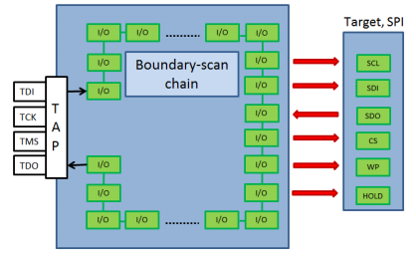
This technique is the easiest, but also the slowest. All the boundary-scan cells (of which there can be thousands in a large FPGA) must be traversed to perform the programming. As a result, programming the memory can take hours for larger programming files. This delay, especially if reprogramming is to be performed frequently, can have a heavy impact on development time.
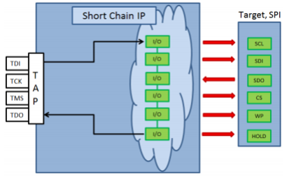
Shortened Boundary-Scan Chain
This programming method involves using ScanWorks FPGA-based Fast Programming (FFP) product to generate an IP module containing a considerably shortened boundary-scan chain (reduced from say, 3,000 cells down to 10-20) which can be used to configure the FPGA, making the programming time much faster.
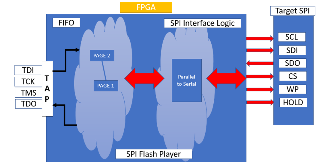
SPI Flash Player IP with FIFO Memory
The most sophisticated method of the three mentioned uses special IP generated by ScanWorks FFP product. ScanWorks FFP includes a SPI Flash Player and page optimization IP which then gets generated to configure the specific FPGA used in the design. Programming data is streamed through an IJTAG network into FIFO memory within the FPGA that matches the page size of the SPI memory device (note that IJTAG is used because of the flexibility of having different test and logic blocks simultaneously instantiated within the FPGA). In parallel, the SPI Flash Player is programming the data into the targeted device. Well-designed IP can achieve the maximum programming speed of the SPI device. As is the case with the shortened scan chain method, the faster programming time realized using the SPI Flash Player IP can significantly reduce delays that impact development time.
Below is a table of real-world customer examples ASSET has collected. The first two examples show the speed of method one, the full boundary-scan chain, compared to method three, the SPI Flash Player IP. The third example compares the speed of the full boundary-scan chain method to the speed of method two, the short-chain:
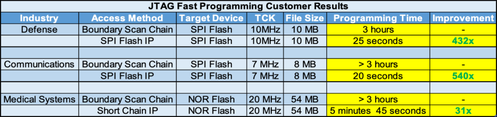
As the data in the table shows, the time savings in terms of production beat rate is dramatic! Time in production is money, so it is easy to see an investment in ScanWorks FPGA-based Flash Programming products pays for itself very quickly.
For more information on the technology behind these methods, see our video of how design and test can work together to achieve the significantly reduced programming time we mentioned in this blog.
https://www.asset-intertech.com/resources/videos/fast-flash-programming-using-fpga-ip/