
Back in 2019, I wrote a four-part series about boundary scan test, demonstrating how JTAG is used to perform basic board structural tests. With the recent (February 15, 2025) 35th Anniversary of JTAG’s ratification by the IEEE, I was motivated to continue the series.
Yes, for those who have been following my recent articles, you’ll know that I’ve written frequently about the use of JTAG for the purposes of “debug”. And I use “debug” in the specific sense of low-level firmware (i.e. UEFI) and software (i.e. operating system, applications) run-control and trace – for example, setting breakpoints, single-stepping through code, etc. But debug in the more general case refers to any sort of troubleshooting: and JTAG first came into existence within the IEEE 1149.1 Standard to perform hardware structural test and debug.
As you’ve probably seen in many articles, JTAG is extremely versatile: it can be used for test, debug, platform validation and device programming.
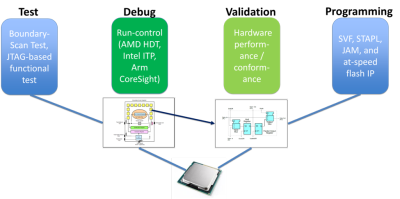
And, in my company, we specialize in using it for all of the above. JTAG operates at such a low level, embedded in so much commercial silicon, that it can do things that cannot be done in any other way. And we’re often called upon to troubleshoot engineering design problems that might originate at the printed circuit level, or in the firmware, or in the operating system, or even in the silicon itself. JTAG tackles the most difficult and impossible problems.
So, in this article, I’ll revisit the use of JTAG for the purpose of boundary scan test of printed circuit boards. I enjoy having fun with our advanced tools, in this case the ScanWorks product.
For background, I’d recommend glancing at the first four articles in my Unboxing Boundary-Scan Test series:
Part 3: More on Scan Path Verify
Part 4: Detecting Faults with SPV
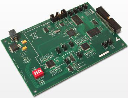
As I resume this series, I graduated to a more recent reference board design of ASSET’s: the ScanLite2 board. This is an updated version of the old original ScanLite board that I used in the first four articles. It’s still a little long in the tooth, but good enough for the purpose of this blog:
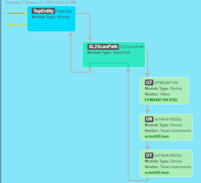
On this ScanLite 2 board, the devices on the board are a little different from that of the ScanLite, and the scan path can be seen in the below block diagram:
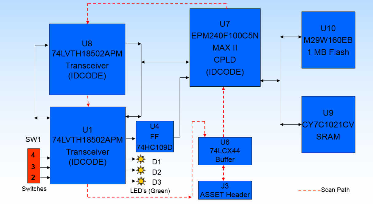
It’s worthwhile looking at the devices in the scan chain, to understand how Scan Path Verify will work on this board. You plug into the J3 connector on the board (which is a “standard” 20-pin header – and I use the term standard loosely) from a ribbon cable originating with a boundary scan hardware controller; in our case, it could be any of ASSET’s controllers: the USB-100, PCIe-410, etc. etc. For now, I’m just using my old reliable USB-100; it’s a single TAP controller, not the fastest hardware controller in the world, but certainly performant enough for basic PCB interconnect testing.
Now, let’s fire up ScanWorks and start testing. In this article, we’ll explore Scan Path Verify, the very first test to create: this validates the hardware connectivity of the board chain, which is essential to doing more advanced tests like interconnect testing or Memory Access Verify (MAV) testing.
In prior articles, I’ve used the example Project in the ScanWorks directory. This example Project helps newcomers get started by having all tests pre-configured. For this article, I’m going to build the SPV test from scratch.
When Launching ScanWorks, we’re prompted to create a new Project, and there’s a new visual aid to the workflow:
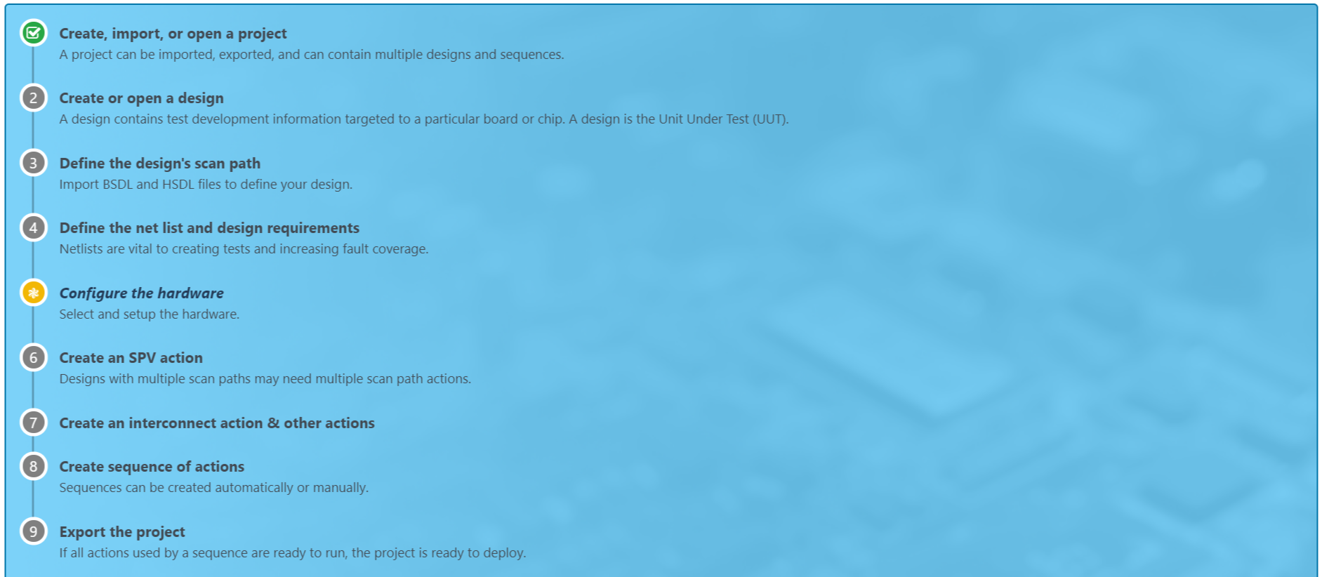
ScanWorks Projects house one or more Designs, which in turn support one or more test Actions. In this case, we’re creating the Designs and Actions with our own knowledge of the ScanLite 2 board. Once the Design is created, we see the a list of things that we can do, that relate back to the workflow:

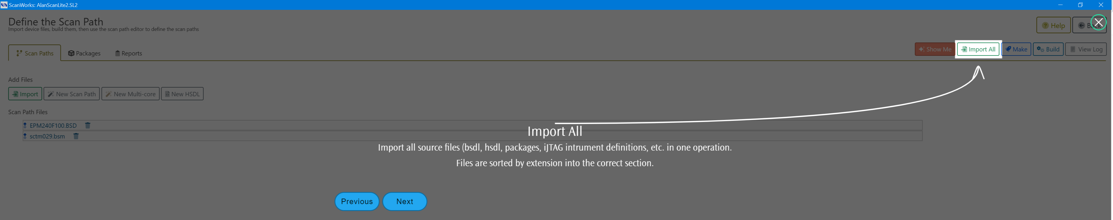
Let’s use the Define the Scan Path under Define the Design up in the left hand corner. And then Import the BSDL files into the Design, which in this case is EPM240F100.BSD for the first device in the scan chain, and then sctm029.bsm for the next two transceivers. Then build the BSDLs to compile them. There’s some nice “Show Me” help available along the way:
Then select New Scan Path to put the devices in the order of the scan chain, be sure to identify the Package Type for each, give them each a Reference Designator (RefDesc, from the netlist or BOM), do a Save and Build, and you’re done. Here’s the visual representation of the scan path:
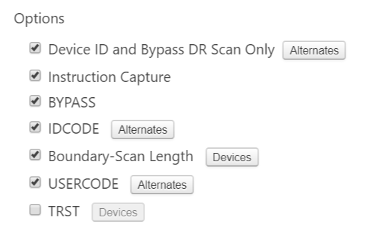
From there, it’s easy to create an SPV Action: click on the Action tab, pick SPV, and then select the Options you’d like to run:
And then run the Action, and here are some Logs that show the results, if you want to see the next level of detail:
********************************************************************************

Project Name: AlanScanLite2

Project Version: 8

Design Name: SL2

Design Version: 7

Action Name: SPV1

Action Version: 2

Run Date: 2/22/2025 2:50:16 PM

********************************************************************************

*** No precondition file present ***

*** Starting DeviceID & Bypass DR scan only test... ***

IDCODE for Device U1 in tap 1 PASSED

   Expected data: 00110000000000011100000000101111

   Measured data: 00110000000000011100000000101111

IDCODE for Device U8 in tap 1 PASSED

   Expected data: 00110000000000011100000000101111

   Measured data: 00110000000000011100000000101111

IDCODE for Device U7 in tap 1 PASSED

   Expected data: 00000010000010100001000011011101

   Measured data: 00000010000010100001000011011101

*** Starting IR Capture test... ***

IR Capture test PASSED for TAP 1

*** Starting BYPASS test... ***

BYPASS test PASSED

*** Starting IDCODE test... ***

IDCODE for Device U1 in tap 1 PASSED

   Expected data: 00110000000000011100000000101111

   Measured data: 00110000000000011100000000101111

IDCODE for Device U8 in tap 1 PASSED

   Expected data: 00110000000000011100000000101111

   Measured data: 00110000000000011100000000101111

IDCODE for Device U7 in tap 1 PASSED

   Expected data: 00000010000010100001000011011101

   Measured data: 00000010000010100001000011011101

*** Starting Boundary Length test... ***

Boundary Length test PASSED for TAP 1.

*** Starting USERCODE test... ***

UserCode for Device U7 in tap 1 PASSED

   Expected data: XXXXXXXXXXXXXXXXXXXXXXXXXXXXXXXX

   Measured data: 00000000000000000000000000000000

Test completed successfully
Interesting, huh? There’s a lot of good information that comes out of the individual tests that give some insight into boundary scan’s internal options, at least for SPV.
Astute readers may ask, you have another device, U6 in the scan path; don’t you have to model this? The answer is no in this instance: U6 is a buffer, and since it by default is in a state that allows it to act transparently (as is fairly standard in the industry) it doesn’t cause problems. On the other hand, if it did cause problems, we would either have to run a precondition macro or a digital IO action to get the board into a state that allows SPV to run unimpeded. This falls into the category of board powerup / conditioning that we have to deal with from time to time.
That’s it for now. There are many aspects of boundary scan test that I’ll be writing about soon. Maybe I’ll tackle Interconnect tests next.
If you want some more background reading on boundary scan, my colleague Michael Johnson has prolifically written many articles on the topic. A 16-part blog series starts with:
Everything You Need to Know About ScanWorks Interconnect Part 1: The Origins of Boundary Scan
and runs through:
Everything You Need to Know About ScanWorks Interconnect Part 12 – Working with a Netlist
Or, for a more complete learning vehicle, read our Boundary Scan Tutorial written by Ben Bales and Adam Ley.